|
Home
| 32KOmnibus
| 4sale
| 8L
| 8a
| 8e
| 8i
| 8s
| C
| FPGA8i
| blog
| cables
| cad
| computerlab
| decmateI
| decmateII
| decmateIII
| df32emul
| documents
| dsd410
| flipchip
| frontpanel
| kc8a
| la36
| lab
| omnibus
| papertape
| pc04
| repair
| rk05
| rl02
| rx02
| rx08
| sbc6120
| software
| tc01
| tools
| tty33
| tty38
| tty43
| ttycards
| tu10
| tu55
| tu56
| typeset
| vt78
|
32K Memory for Omnibus
Some of you have asked, so here is a shortcut to the CAD drawings.
|
Of these, the "Lafferty1" drawings are the board as sent off for fabrication, and the "Lafferty1ab" (as built) drawings are the board as it looks if you bought a kit and built it as recommended.
|
Here are some assembly hints for the Omnibus memory (click any photo for a larger version):
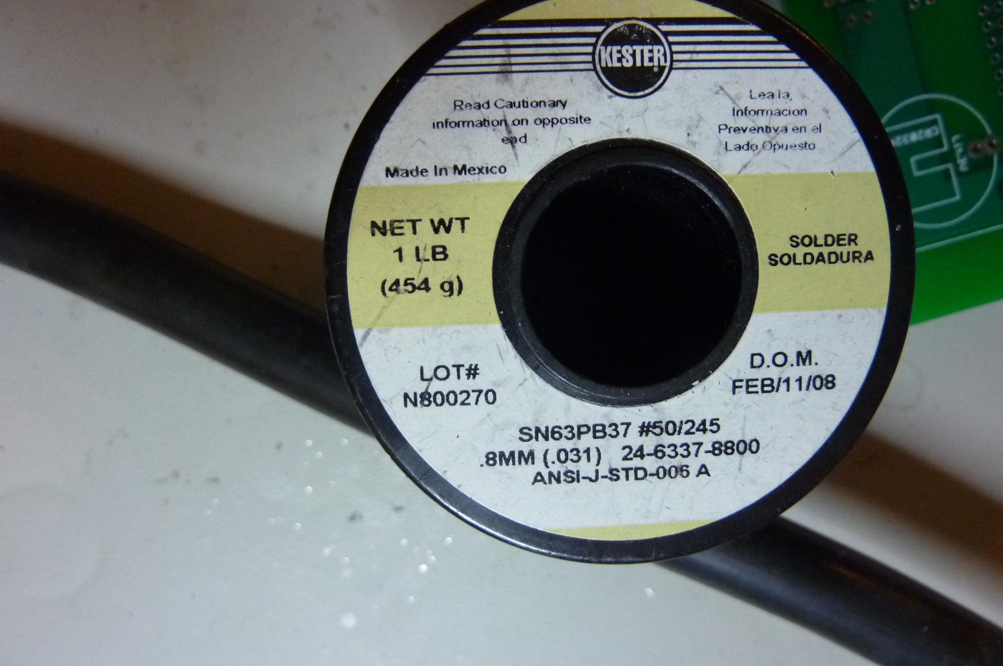
I use eutectic (63/37) no-clean rosin core solder in the 0.031 inch (0.8mm) thickness, and a fairly hot iron (325 degrees), for an easier soldering experience. The boards come in a tin-lead finish, so soldering this is about as easy as soldering gets. |

Here are the parts kits, all sitting in a box. You should get one snack-size ziploc with the discretes, one anti-static bag with chips and sockets, and a board, for each kit you have ordered. You should also get a printed sheet with the most important release notes as of wheever your board was shipped. |
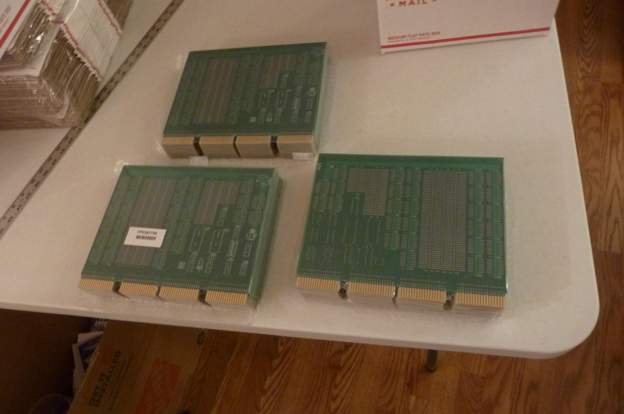
Here are the boards in their shrink-wrap, as received from the board shop. |


The front and back sides of the boards. The front side is the one with the components marked, and also is the side from which the components are inserted. |

Start out by inserting the largest IC sockets. Pin one goes on the end with a notch, so point the notch away from the edge connectors, as shown. Flip the board over and tack-solder diagonally opposite sides of the socket. Then pick up the board, and while pressing down gently on the socket, reheat the solder so that it is tacked as far into the board as it wants to go. (Don't burn your fingers!) Then finish soldering the socket into place. One note about these sockets. They are machine pin sockets, but the contacts aren't gold -- they are tin/lead. I think they are fine, but if you really wanted the gold ones, you'll have to provide them yourself (they are about twice the price of these). |
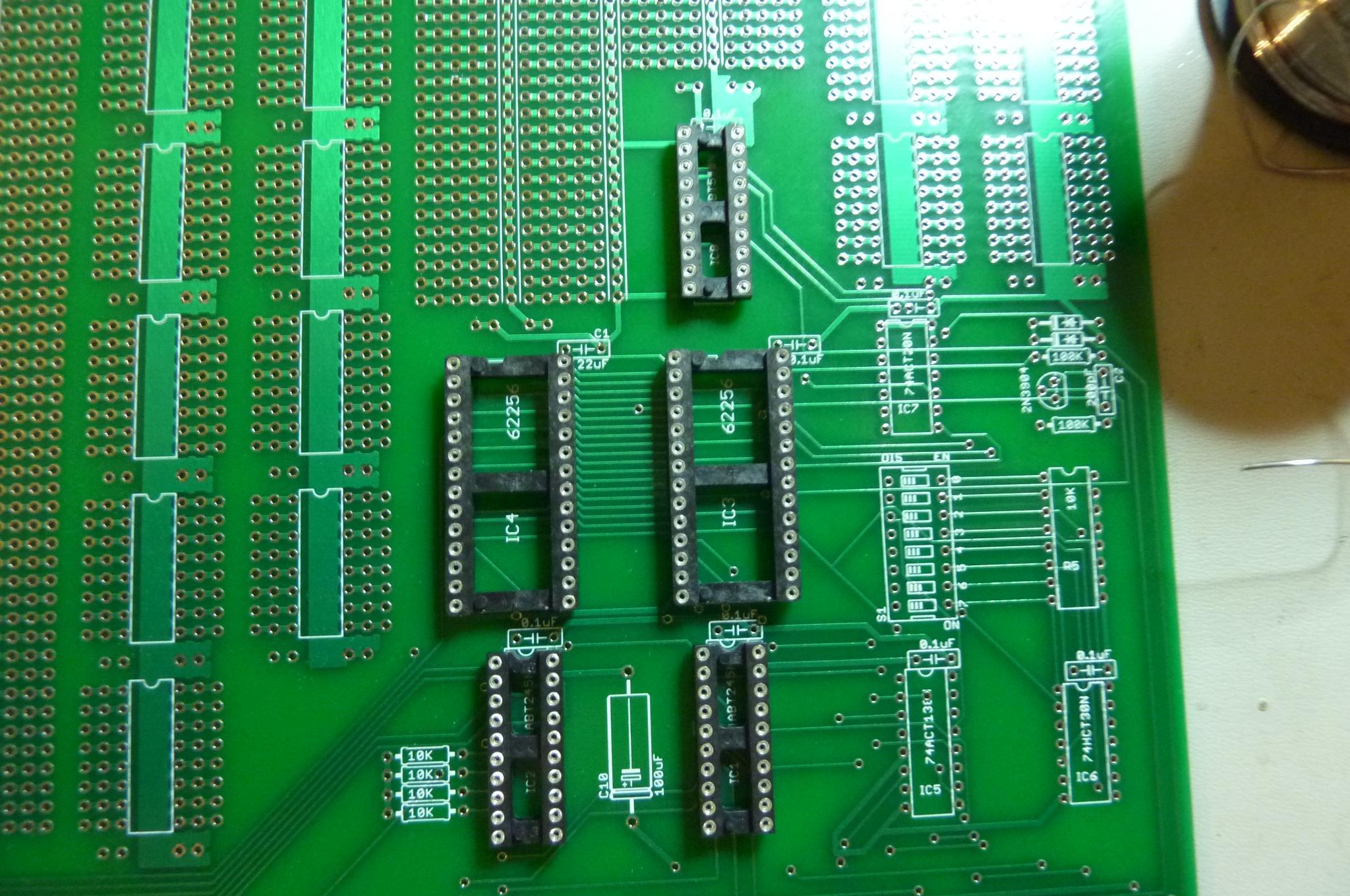

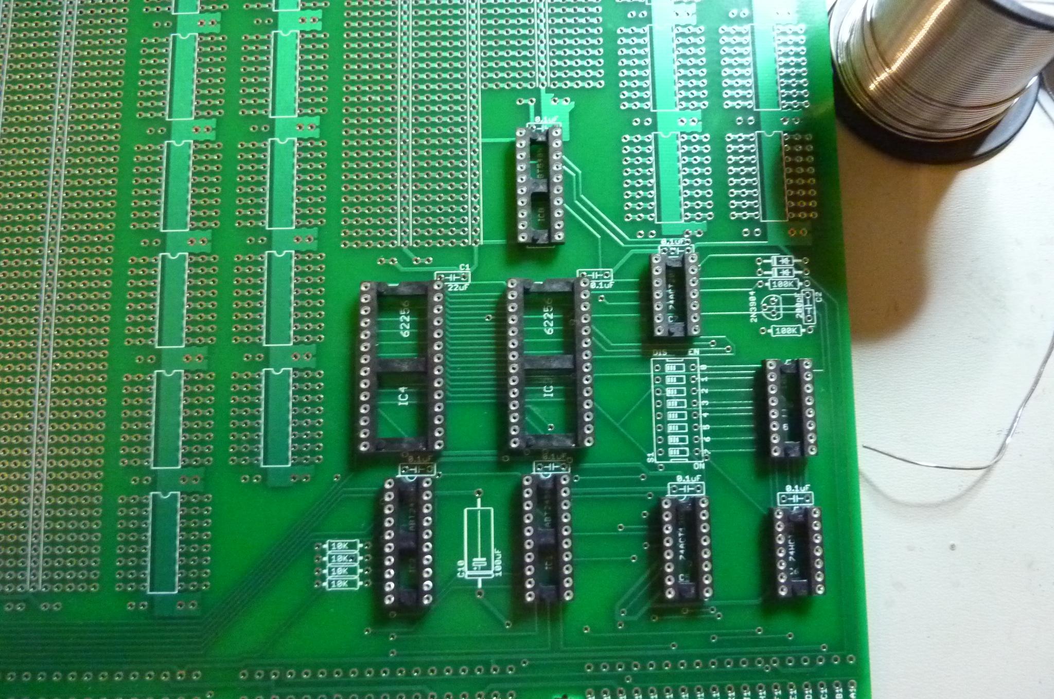
Work your way through the successively smaller IC sockets. Working from large to small ensures you don't solder (for instance) a 14 pin socket into a place where the 16 pin socket should be. |
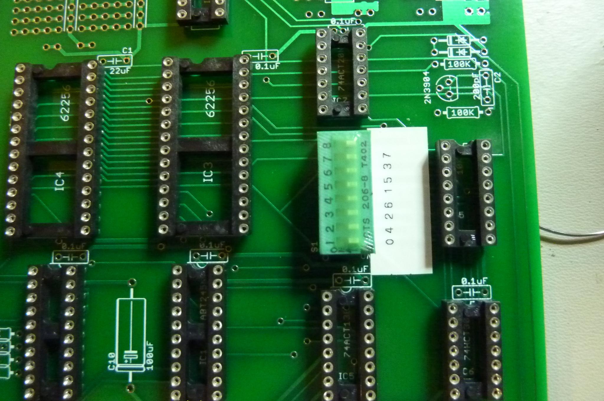
Solder in the DIP switch. The orientation shown will correctly make the "disabled" position to the left. The silkscreen is wrong about the dip switch orientation, and also about the ordering of the banks. I've made a little sticker which numbers the banks to match the actual implementation. It is also possible to cut traces and install blue wires to interchange pin 1 and pin 3 of IC5 (which is just below the DIP switch). This should make the switches correspond to the banks as indicated by the silk screen. |

Solder in the electrolytic. This is a polarized component, so be sure that the "-" end is away from the edge connector, and the ridged end is toward them, as shown. Bend the long leads slightly after inserting, so that the part doesn't fall back out. Trim the leads after soldering. |
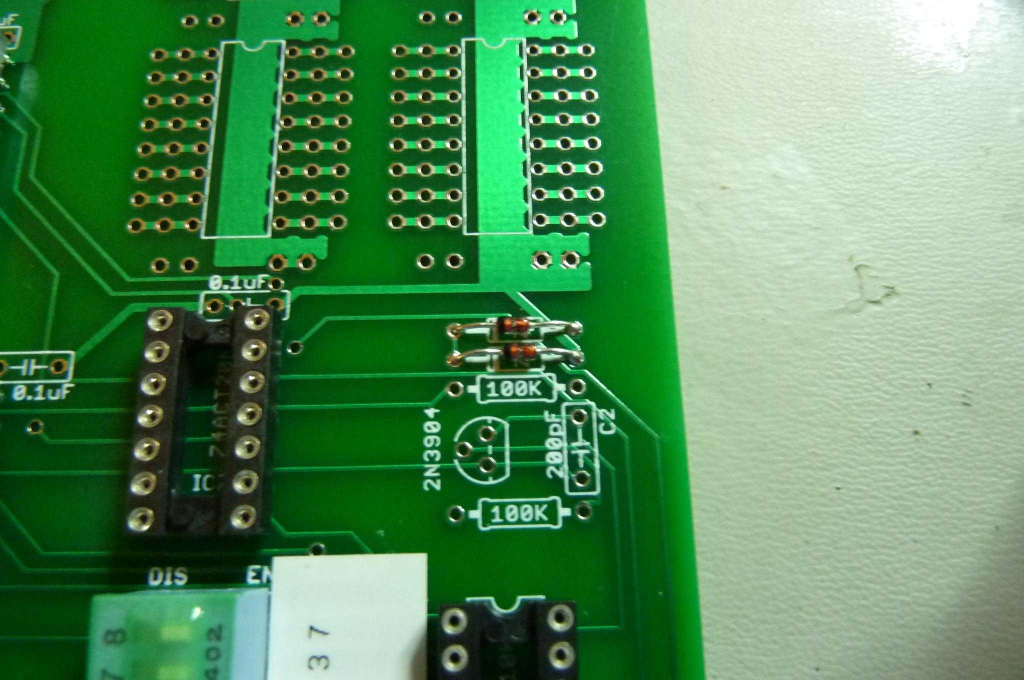
The Schottky diodes are also polarized components. Solder them with the black side (cathode) to the left, as shown. |

At this point I went ahead and soldered in the non-polarized capacitors, paying attention to which value goes in which spot. I like to orient the markings on the components to match the markings on the silkscreen. |


The 10K (orange stripe) resistors go on the left, and the 100K (yellow stripe) resistors go on the right. |

If you plan to install the board in an 8/A, you'll find there is an interference fit (upper pic) between the battery holder and the card guides. One solution to that problem can be found here. Alternatively, you can substitute JameCo part #355434, which does not have the problem (lower pic). I can furnish you with the JameCo part upon request. |


The battery holder goes as shown (8/A version in lower pic). Be sure to get it flat to the board, and yes, the "+" lead hole is oversized. You might also need a little more heating time to make sure these don't end up with cold solder joints. Be sure to trim the "+" lead flush when you are done. |

It wasn't really necessary to delay putting in the transistor, but I wanted to double check it's orientation. It looks like the way it is drawn in the silkscreen is correct for the transistor provided. Bend the center lead back gently to get it into the hole. |

That's basically it for the soldering. |

Insert the various chips. Be sure to get the right chips into the right sockets, with pin one pointing away from the edge connectors. The chips are a little static sensitive (it shortens the life of the chips), so don't work in an environment where static electricity can build up, and try to minimize handling. To get the chips in, place the chip on it's side on the board, and rock it slightly, bending all the pins at once until they point more or less straight down from the chip body. Place the chip in it's socket (pin 1 away from the edge connectors!), and make sure then thin part of each pin is started in the socket hole before applying pressure. When everything is looking good, press firmly on the chip body to press the pins into the grippers inside the holes. You should be able to tell when it is seated. |

Insert the battery from the left, writing side up, and press down until the plastic tab on the left clicks over the top of the battery. |

Lastly, you may wish to cover the exposed "+" battery wiring at the battery terminals and at the diodes with a couple of layers of non-conductive tape. This limits the likelyhood of shorting the battery when setting the board down. If you want to be completely paranoid about it, cover pin 28 of IC3 and IC4, too. (Sorry, no handles come with your kit.) |

You've done it! |
|
Last updated on 02/25/23 02:21 |
||||||||||||||||